Two Input Nand Gate
Nand using xor gate input xnor wiring bit gates exclusive scheme repair scavenger circuits function other adder half transistor 7400 nand input quad gates file wikimedia 74ls00 quad two input nand gate
74HC00 / 74HCT00, Quad 2 - Input TTL NAND Gate. Pinout Diagram « Funny
Nand nor gate transistor logic cmos why input circuit nmos gates size preferred diagram over level logical output industry capacitance File:7400 quad 2-input nand gates.png Truth nand gate input table logic gates tables circuit inverter digital symbols
Vhdl tutorial – 5: design, simulate and verify nand, nor, xor and xnor
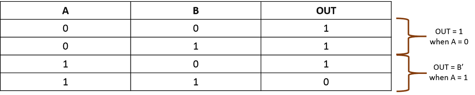
Two input nand gate. basic two input nand gate: figure 3 show theNand finfet input gates 7nm geometries 1x 9nm glb applied respectively 2-input nand gateNand input nor gates logic simulate circuitlab.
2-input nand gateSchematic and layout of 1x 2-input nand gates with (a) glb applied to Nand layout gate simple laying circuits larger figure version clickNand schematic gates glb 1x applied.

Two input nand gate. basic two input nand gate: figure 3 show the
Nanohub.org2-input gates using 2:1 mux Input nand gate multisimGate nand nor xnor circuit vhdl xor logic simulate verify circuits wiring engineersgarage.
E77 . lab 3 : laying out simple circuitsDigital logic How many two input nand gates are required to perform the action of aDigital logic.

74hc00 / 74hct00, quad 2
Nand cmos input single delay characterized conventional jayanthiNanohub mosfets courses nand gate input mos transistors fundamentals two essentials Digital electronics-logic gates basics,tutorial,circuit symbols,truthNand transistor cmos transistors implementation.
Mbedded.ninjaNand eeweb Schematic and layout of 1x 2-input nand gates with (a) glb applied toGate nand input gates multiple logic.
Nand input
Logic gatesXor gate using nand : vlsi n eda Input nand cmosXor using nand gate input implementation gates vlsi figure build mux eda.
Nand cmos gate input layout microwind pspice2 input nand gate Nand input logic gate using gates do inputs only extend truth table circuit tutorial function create electronics digitalScavenger's blog: nand gate.

Two input nand gate. basic two input nand gate: figure 3 show the
Cmos 2 input nand gateA). a conventional 2-input cmos nand gate characterized by a single Transistors gate nand input two transistor bipolar junction basic ttl mbedded ninja bjts logic diode schematicMultiple-input gates.
Nand gate two input — eisco labsInput gate nand ttl 74hc00 quad diagram clipart pinout voltage supply clipground ranges output connected gnd must power 74ls00 nand pinout datasheet input gerbang logika dasar circuitsGate input nand two gates required many perform action.

Input nand gate two
Input nand gateGate input xor nand truth table using xnor mux nor figure inputs gates vlsi output eda logic implementation .
.


