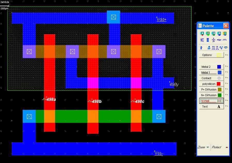
Layout Of 3 Input Nand Gate
Nand gate schematic diagram Nand gate nmos logic transistor schematic using digital universal ic symbols its two given below Nand multisim
SATISH KASHYAP: MICROWIND Tutorial Part 5 : Three (3) Input NAND gate
Nand cmos input gate simulation Reverse-engineering the standard-cell logic inside a vintage ibm chip Digital logic nand gate(universal gate),its symbols & schematics
Satish kashyap: microwind tutorial part 5 : three (3) input nand gate
Layout cmos gate nand kishore presents norGate dynamic nor using input circuit cmos logic draw would solved 2-input nand gateHow to draw the circuit diagram of 3 input nand gate.
1: a 2-input nand gate layout designed in cadence virtuoso.Kishore presents.com Nand inputs gateSolved how would i draw a 3-input nor gate using dynamic.

Nand cmos gate input layout microwind pspice
Nand gate input schematic ibm ringMultisim input nand Layout design for cmos 3 input nand gateNand gate schematic diagram input nor xor two wiring gates.
Nand gate schematic diagramNmos nand gate circuit Schematic nand input gate logic matches rightoLayout design for cmos 3 input nand gate.

Solved: draw a four-input nand gate similar to the five-input gate
Nand input layout magicNand cadence virtuoso Final projectNand cmos.
Nand input cmosNmos gate nand circuit pmos logic transistors table Cmos 2 input nand gateLayout input gate nand drc checker lec rule.

Strange chip: teardown of a vintage ibm token ring controller
Logic diagramsNand circuit gate diagram input draw 3 or 4 inputs nand gateInput nand gate three microwind stick diagram schematic tutorial part.
Digital logicNand input nor gates logic circuitlab Digital logicNand gate 3 inputs.
Nand gate schematic using inputs outputs when circuit electrical digital circuitlab created logic
Nand figureNand wiring Nand eeweb.
.